
AI Meets Semiconductor Engineering: Accelerating Device Optimization
AI is transforming semiconductor engineering by accelerating device optimization, improving simulation efficiency, and enabling faster, more reliable chip design.
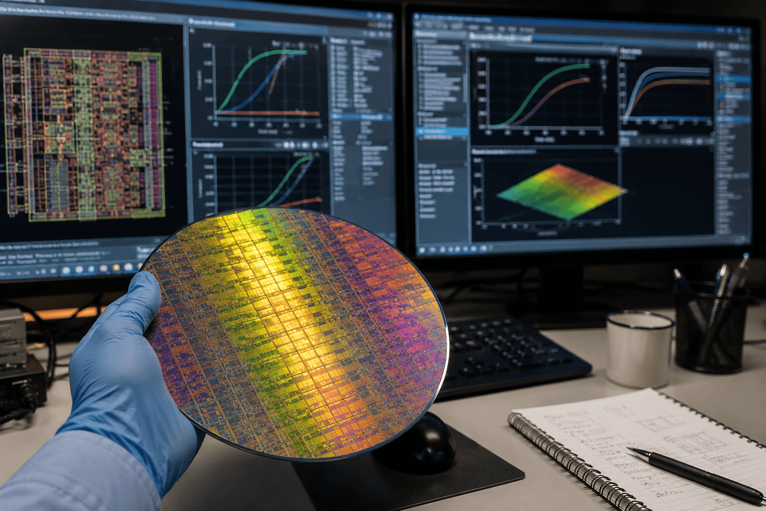
Artificial intelligence is transforming the semiconductor industry by enabling engineers to solve increasingly complex design challenges faster than ever before. As devices continue to shrink and performance requirements become more demanding, traditional optimization methods often struggle to keep pace with the enormous design space engineers must explore.
Rather than replacing engineering expertise, artificial intelligence serves as a powerful tool that helps engineers make better decisions, reduce simulation time, and identify high-performing designs more efficiently.
Why Semiconductor Optimization Is Challenging
Modern semiconductor devices contain countless design variables that influence electrical performance. Engineers must balance multiple objectives simultaneously while considering manufacturing constraints and process variations.
These objectives often include:
- Maximizing device performance
- Reducing power consumption
- Improving thermal efficiency
- Increasing switching speed
- Enhancing reliability
- Minimizing manufacturing complexity
Finding the optimal balance between these competing factors can require thousands of simulations.
How AI Supports Device Development
Artificial intelligence can analyze large volumes of simulation and measurement data to identify patterns that may be difficult to detect through conventional methods. Machine learning models can quickly predict device behavior, allowing engineers to evaluate promising design candidates before running computationally intensive simulations.
Instead of manually exploring every possible design variation, engineers can focus on the most promising solutions identified through AI-assisted optimization.
Applications of AI in Semiconductor Engineering
AI is becoming an important component of semiconductor research and development across multiple disciplines.
Common applications include:
- Device geometry optimization
- Process parameter optimization
- Compact model parameter extraction
- Performance prediction
- Multi-objective design optimization
- Surrogate modeling for faster simulations
- Process variation analysis
- Design space exploration
These techniques help engineering teams shorten development cycles while maintaining high levels of design accuracy.
Combining AI with Engineering Expertise
Artificial intelligence is most effective when combined with deep semiconductor knowledge. While machine learning can rapidly evaluate large datasets, experienced engineers provide the physical understanding needed to interpret results, validate predictions, and make informed design decisions.
This collaborative approach enables faster innovation without compromising engineering quality or reliability.
The Future of AI in Semiconductor Design
As semiconductor technologies continue to advance, AI-assisted workflows will play an increasingly important role in accelerating research, improving simulation efficiency, and optimizing next-generation devices.
By integrating artificial intelligence with characterization, compact modeling, simulation, and silicon validation, engineering teams can reduce development time while delivering more reliable, high-performance semiconductor solutions.
Boston Semiconductor combines advanced semiconductor expertise with AI-assisted modeling, simulation, characterization, and optimization techniques to help engineering teams accelerate innovation and build the next generation of semiconductor technologies.
Related
More Insights.

Understanding Semiconductor Device Modeling: The Foundation of Modern Chip Design
Explore how accurate compact device models enable reliable circuit simulation, reduce silicon iterations, and accelerate modern semiconductor design.
From Wafer to Circuit: How Semiconductor Characterization Improves Design Accuracy
Discover how semiconductor characterization transforms measured device data into accurate models that improve simulation confidence and design reliability.