
Understanding Semiconductor Device Modeling: The Foundation of Modern Chip Design
Explore how accurate compact device models enable reliable circuit simulation, reduce silicon iterations, and accelerate modern semiconductor design.

Every advanced semiconductor begins with an accurate device model. Before a chip is fabricated, engineers rely on mathematical representations of transistors to predict how circuits will behave under different operating conditions. These compact models enable designers to simulate performance, identify potential issues, and optimize designs long before manufacturing begins.
As semiconductor technologies continue to evolve, accurate device modeling has become an essential part of reducing development costs, minimizing design iterations, and accelerating time to market.
What Is Semiconductor Device Modeling?
Semiconductor device modeling is the process of creating mathematical models that represent the electrical behavior of transistors and other semiconductor devices. These models are used by electronic design automation (EDA) tools to simulate integrated circuits without requiring physical prototypes.
By accurately representing real device behavior, engineers can evaluate circuit performance during the design phase and make informed engineering decisions.
Why Accurate Models Matter
Even small inaccuracies in a device model can lead to unexpected circuit behavior after fabrication. Reliable compact models help engineering teams predict real-world performance with greater confidence.
Key benefits include:
- Improved simulation accuracy
- Reduced costly silicon revisions
- Faster product development
- Support for analog, RF, and mixed-signal design
- Greater confidence before tape-out
The Role of Characterization
Device models are only as accurate as the data used to create them. Semiconductor characterization measures electrical behavior across different operating conditions, including voltage, temperature, and process variations.
This measured data forms the foundation of high-quality compact models that closely represent fabricated devices.
From Silicon to Simulation
A modern modeling workflow typically includes several key stages:
- Device characterization
- Data analysis
- Compact model extraction
- Model validation
- Silicon correlation
- Version-controlled model release
Each stage helps ensure that simulation results closely align with actual silicon performance.
Looking Ahead
As semiconductor devices become more complex and new materials such as gallium nitride (GaN) and silicon carbide (SiC) gain wider adoption, the importance of accurate device modeling continues to grow.
Organizations investing in robust modeling and validation workflows can reduce development risk, improve design quality, and accelerate innovation across the semiconductor industry.
Boston Semiconductor provides advanced semiconductor modeling, characterization, validation, and simulation solutions that help engineering teams develop reliable, high-performance integrated circuits with confidence.
Related
More Insights.
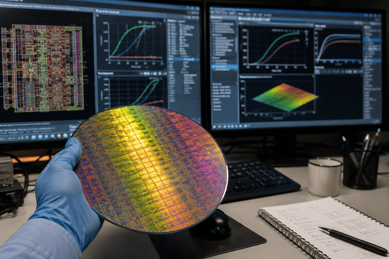
AI Meets Semiconductor Engineering: Accelerating Device Optimization
AI is transforming semiconductor engineering by accelerating device optimization, improving simulation efficiency, and enabling faster, more reliable chip design.
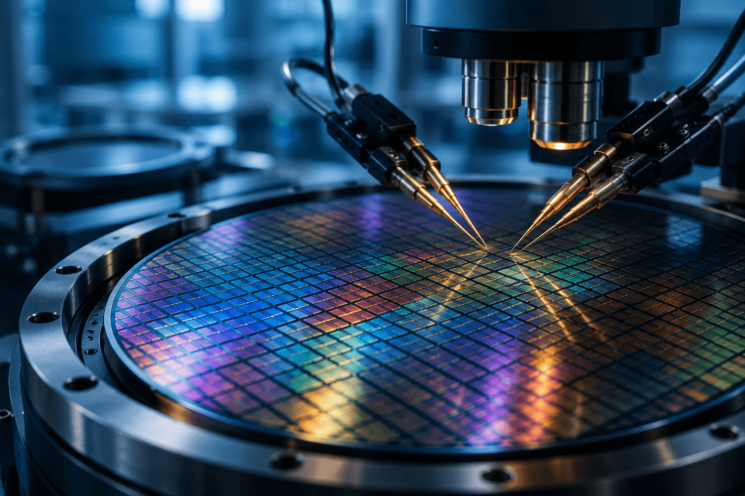
From Wafer to Circuit: How Semiconductor Characterization Improves Design Accuracy
Discover how semiconductor characterization transforms measured device data into accurate models that improve simulation confidence and design reliability.