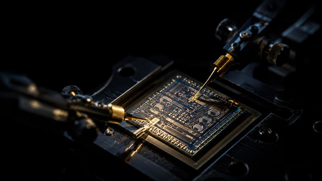
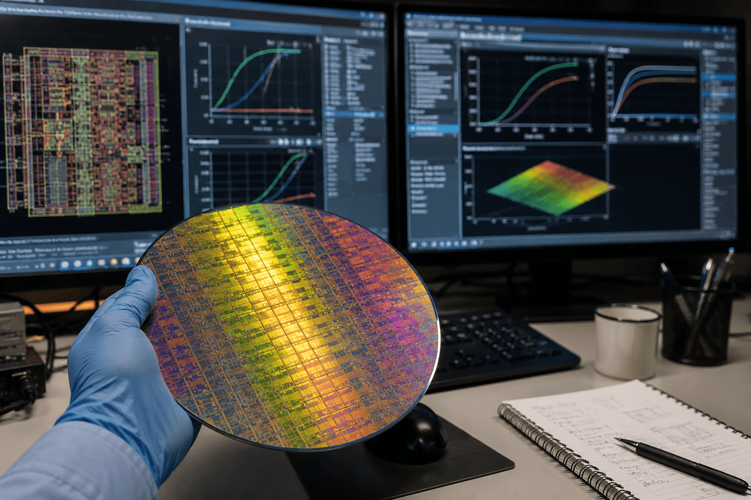
Full-stack semiconductor design capability, mapped the way our engineers actually think about a chip.
// 01
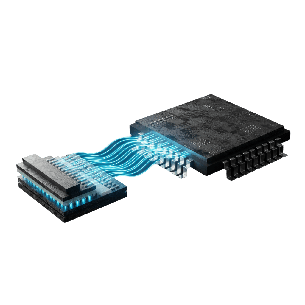
3D-IC Design
Advanced 3D integration, chiplet architecture, die-to-die interfaces, and TSV design for next-gen packaging.
// 02
Silicon Photonics
Photonic IC design and integration services spanning waveguides, modulators, and electronic-photonic co-packaging for high-bandwidth optical interconnect.
// 03
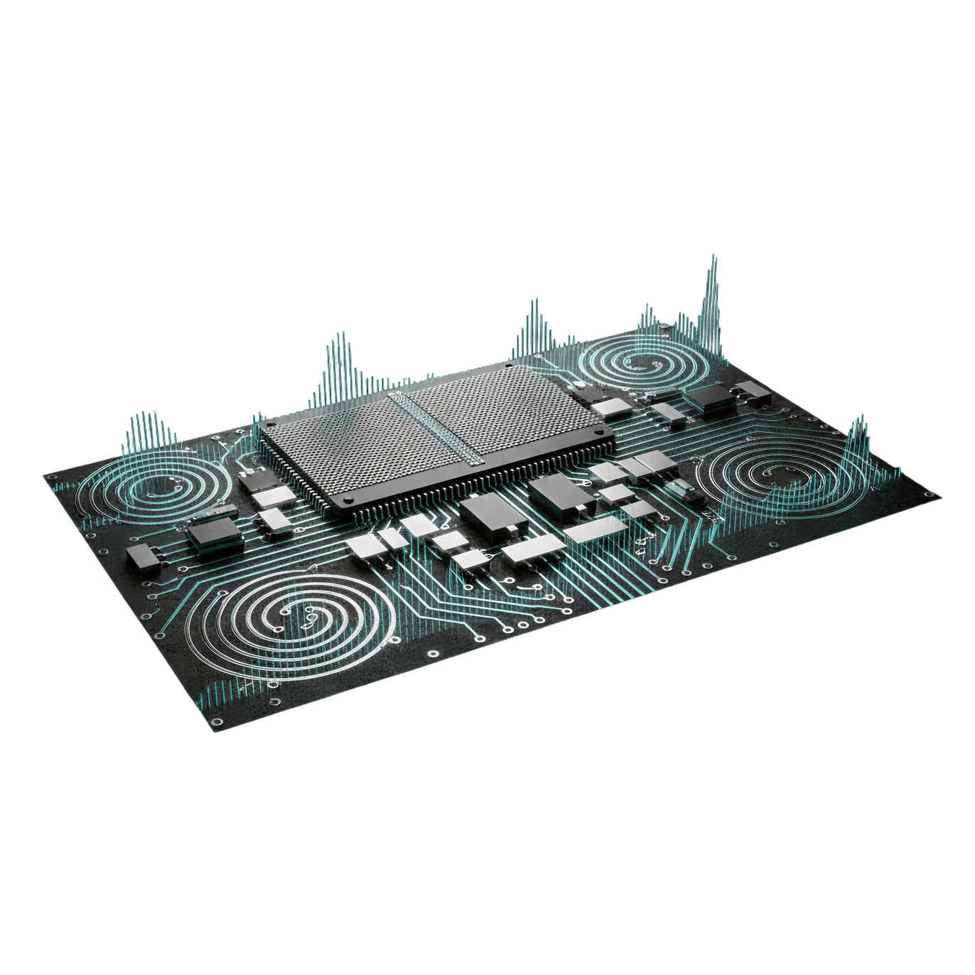
RF & Analog
Transceivers, PLLs/synthesizers, and high-speed analog interfaces for 5G, Wi-Fi, automotive, and IoT applications.
// 05
TCAD Simulation
Process and device simulation, PDK calibration, and SPICE model extraction using Sentaurus TCAD and Silvaco Atlas/Victory.
// 04
Quantum Computing
Design and engineering support for quantum hardware — from cryo-CMOS control circuitry to qubit interconnect and packaging challenges unique to sub-Kelvin operation.
// 06
Physical Design
Full RTL-to-GDSII implementation — synthesis, floorplan, CTS, routing and signoff on nodes down to 3nm.
// 07
AMS Verification
Our modeling team delivers deep expertise in analog behavioral modeling and AMS (Analog Mixed-Signal) verification for complex analog IPs. We enable early mixed-signal validation, reducing verification cycles while improving design-to-silicon confidence.
UNDER THE FLOORPLAN
How each block actually gets built.
The toolchains, nodes, and signoff criteria behind each service area.
Device physics through to power stage.
We design high-electron-mobility transistors (HEMTs) across GaN-on-Si and GaN-on-SiC processes — from gate driver co-design to thermal reliability analysis. Every device is simulated end-to-end with SPICE models calibrated to foundry PDKs, targeting EV chargers, telecom, and 5G power stages.
HEMT design · GaN-on-Si & GaN-on-SiC
Process simulation via Sentaurus TCAD & Silvaco Atlas
I-V, C-V, transient & AC device analysis
SPICE extraction calibrated to foundry PDKs
Advanced-node PnR, signed off.
Full RTL-to-GDSII implementation from synthesis through DRC/LVS signoff, across nodes from 3nm to 90nm using Synopsys Fusion Compiler, Cadence Innovus, and ICC2. Low-power flows with multi-Vt, power gating, and UPF/CPF — plus 3D-IC chiplet integration including UCIe, HBM, and EMIB die-to-die interfaces. 10+ tapeouts delivered.
RTL-to-GDSII · Synopsys FC · Cadence Innovus · ICC2
Nodes: 3nm, 5nm, 7nm, 14nm, 28nm → 90nm
Low-power: multi-Vt, power gating, UPF/CPF
Chiplet integration: UCIe · HBM · EMIB · TSV
RF-aware, parasitic-sensitive layout.
Proven expertise across LNAs, PAs, mixers, VCO/PLLs, and full transceiver front-ends — verified via HFSS and Momentum/ADS EM simulation. We cover HDMI, MIPI, USB3.x, and PCIe analog interfaces, SerDes AFE, LVDS/DDR/LPDDR comboPHY, and 5G communication chip IP modules, all built with parasitic-sensitive custom layout at the core.
LNA · PA · Mixer · VCO/PLL · Synthesizer design
Full TX/RX transceiver front-end architecture
SerDes AFE · LVDS/DDR/LPDDR comboPHY
EM simulation: HFSS & Momentum/ADS
ENGAGEMENT MODELS
Two ways to work with us.
Flexible delivery structures, built around how chip projects actually run.
// RETAINER-BASED
Dedicated team, monthly
Allocation
Senior engineers, assigned monthly
Scope
Task-driven — bugs, reviews, new features
Billing
Predictable monthly, easy to scale
Best for
Ongoing support & maintenance
// TURNKEY
Fixed scope, spec to silicon
Delivery
Complete spec → GDSII / silicon
Payments
Milestone-based — spec, RTL, tapeout
IP terms
Work-for-hire — client owns all IP
Best for
New products & time-critical tapeouts
IP SECURITY
Your IP never leaves the ODC.
Enterprise-grade protection at our Bangladesh offshore development center.
IP & Legal
NDA signed by all personnel
Work-for-hire — client owns IP
Export regulation adherence
Device & Data
Air-gapped RTL/Netlist/GDS machines
Full-disk encryption, EDR tools
No BYOD — company devices only
Access Control
Biometric ODC room access
MFA on all engineering systems
Role-based version control
Secure Communication
Encrypted VPN to client servers
24/7 ODC surveillance
Dedicated Bridge Engineer
FULL-STACK
One team, one partner
From TCAD device physics to physical verification signoff - no handoffs between vendors.
ADVANCED NODE
Proven on leading nodes
Tapeouts on TSMC 3nm–28nm, Samsung 5nm, and GlobalFoundries processes.
WHY BOSTON SEMICONDUCTOR
Built for chip teams that can't afford a leak.
IP-SAFE
Air-gapped delivery
Biometric ODC access and strict NDAs - your IP never leaves our secure environment.
COMMERCIAL
Flexible terms
Retainer or turnkey - we adapt to your project structure and budget.
TRACK RECORD
Silicon-validated
10+ tapeouts and proven analog IPs, recognized at BEAR 2025.